PCB Materials

Home / PCB Materials

PCB Materials

Printed circuit board is the most important part of electronics. Alternately, the acronym has also accounted for printed wiring boards and printed wiring cards, which are essentially the same thing. Due to the crucial role of these boards in everything from computers to calculators, PC board material selection should be undertaken with care and knowledge for electrical necessities of a given piece of equipment.

Before the development of the PCB, circuit board materials were mostly covered by nests of entangled, overlapping wires that could easily fail at certain junctures. They could also short circuit once age took hold and certain wires started to crack. As could be expected, the manual process that went into the wiring of these early boards was confusing and painstaking.

As an increasing variety of everyday electronic components began to rely on circuit boards, the race was on to develop simpler, more compact alternatives, and this led to the development of the material, PCB. With PCB materials, circuits can be routed between a host of different components. The metal that facilitates the transfer of current between the board and any attached components is known as solder, which also serves a dual purpose with its adhesive qualities.

PCB Material Composition

PCB generally consists of four layers, which are heat laminated together into a single layer. The material used in PCB from top to bottom includes Silkscreen, Soldermask, Copper and Substrate.

The last of those layers, substrate, is made of fiberglass and is also known as FR4, with the FR letters standing for “fire retardant.” This substrate layer provides a solid foundation for PCBs, though the thickness can vary according to the uses of a given board.

A cheaper range of boards also exist on the market that don’t utilize the same aforementioned PCB materials, but instead consist of phenolics or epoxies. Due to the thermal sensitivity of these boards, they tend to lose their lamination easily. These cheaper boards are often easy to identify by the smell they give off when being soldered.

PCB second layer is copper, which is laminated onto the substrate with a mixture of heat and adhesive. The copper layer is thin, and on some boards there are two such layers – one above and one below the substrate. PCBs with only one layer of copper tend to be used for cheaper electronics devices.

The massively-used copper clad laminate (CCL) can be classified into different categories according to different classification standards including reinforcing material, used resin adhesive, flammability, CCL performance. The brief classification of CCL is shown in the following table.


Reinforcing Material
Classification Standard Material
Paper base class PF resin (XPC, FR1, FR2) Epoxy resin (FE-3) Polyester resin
Glass fiber cloth base class Epoxy resin (FR4, FR5)
Composite epoxy material (CEM) /
Lamination multilayer base class /
Special material base class BT, PI, PPO, MS
Flammability
Classification Standard Material
Flame-proof type UL94-VO, UL94-V1
Non-flameproof type UL-94-HB
CCL Performance
Classification Standard Material
CCL with ordinary performance /
CCL with low dielectric constant /
CCL with high heat resistance /
CCL with low coefficient of thermal expansion /

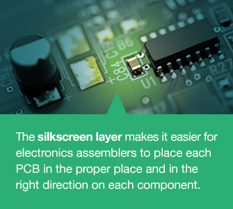
Above the green soldermask is the silkscreen layer, which adds letters and numerical indicators that make a PCB readable to tech programmers. This, in turn, makes it easier for electronics assemblers to place each PCB in the proper place and in the right direction on each component. The silkscreen layer is usually white, though colors such as red, yellow, gray and black are also sometimes used.

Why silkscreen layer | PCBCart

PCB Layer Technical Terms

Besides knowing how PCB is layered, you should know technical terms accompanies the use of PCBs:

  • Annular ring. The copper ring that surrounds the holes on a PCB.
  • DRC. An acronym for design rule check. Essentially, DRC is a practice whereby the design of a PCB is checked for its functionality. Details that are checked include the width of the traces and drill holes.

Design Rule Check | PCBCart

  • Drill hit. Used to describe all holes on a PCB, whether correct or misplaced. In some cases, a hole might be slightly incorrect due to dull drilling equipment used during the production.
  • Finger. Metal exposed along the board edge that serves as connecting points between two PCBs. Fingers are most often found on old video games and memory cards.
  • Mouse bits. A PCB section overly drilled to the point where it threatens the board’s structural integrity.
  • Pad. An area of exposed metal on a PCB, onto which a soldered piece is generally applied.
  • Panel. A large circuit board consisting of smaller boards, which are eventually separated for individual use.
  • Paste stencil. A metal stencil on a board, onto which paste is placed for soldering.
  • Plane. A larger section of exposed copper on a PCB, which is marked by borders but lacks a path.
  • Plated through hole. A hole that goes straight through a PCB, usually for the purpose of connecting another component. The hole is plated and usually features an annular ring.
  • Slot. Any hole that isn’t circular. PCBs with slots are often high priced due to the production costs of creating odd-shaped holes on a circuit board. Slots are typically not plated.
  • Surface mount. A method whereby external parts are mounted directly to PCB without through holes.
  • Trace. An ongoing line of copper across a PCB.
  • V-score. A place where the board has been partially cut. This can render a PCB vulnerable to snapping.
  • Via. A hole through which signals travel between layers. Tented versions are covered with protective soldermask, while the untented vias are used for connector attachments.

The number that precedes a layer refers to the exact number of conducting layers, be it a routing or plane layer – the two layer types. Layers tend to have the number 1, or any of the next four even numbers: 2, 4, 6, 8. Layer boards sometimes have odd numbers, but these are rare and would make hardly any difference. For example, the PCB material in a 5 layer or 6 layer board would be virtually identical.

Conducting Layer Types | PCBCart

The two layer types have different functions. Routing layers feature tracks. Plane layers serve as power connectors and feature copper planes. Plane layers also feature islands that determine the signaling purpose of a board, be it 3.3 V or 5 V.

FR4 is code name for glass-reinforced epoxy laminated sheets. Due to its strength, as well as its ability to withstand moisture and fire, FR4 is one of the most popular PCB materials.

Additional PCB Design Considerations

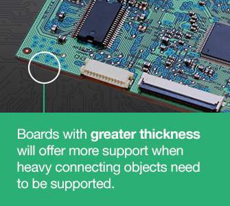
A figure such as 1.6 mm is used to indicate the thickness of a layer board. On 4 layer boards, 1.6 mm is the standard measure. Boards with greater thickness, for example, will offer more support when heavy connecting objects need to be supported.

The standard level of copper thickness on plane layers is 35 microns. Alternately, copper thickness is sometimes indicated in ounces or grams. It’s best to go for higher than normal copper thickness on boards that support a lot of applications.

PCB Board Thickness Choice | PCBCart

Tracks aren’t meant to transfer power, but this can sometimes happen when signals don’t properly handle frequencies. If the problem isn’t kept in check, the tracks could end up losing major amounts of power. To get as much power as possible moved from one side of a track to the other, the layout of the track must account for transmission equations.

Generally, two inches is the right track distance on layer boards that consist of copper-tracked FR4 PCB material, providing that the signal time is one nanosecond. However, you must consider the effects of transmission line for high track lengths, particularly if signal integrity is crucial. The Internet is full of programs and spreadsheets that are designed to help people make proper impedance calculations for specific layer boards.

On most boards, vias are empty, and you can usually see right through them. Nonetheless, there are various circumstances under which vias can be filled. For starters, it’s necessary for the vias to be filled when it comes to forming protective barriers from dust and other impurities. Secondly, vias might be filled to boost the carrying capacity of a current, in which case conducting materials might be used. Another reason that vias might be filled is to level a board.

Vias are typically filled with ball grid array (BGA) pieces. If contact occurs between a BGA pin and an inner layer, solder could slip through the via and onto a different layer. Therefore, the vias are filled to ensure solder doesn’t leak to another layer, and the integrity of contacts are maintained as intended.

One of the more troublesome occurrences on a layer board is when a contact breaks in and out at some point along the board. The more this happens, the sooner that part of the board is liable to give out entirely. The average home electronics user will experience this problem when one of the buttons on a calculator stops working. Each button presses down on a particular part of a layer board, and when one spot gets faulty, the button that correlates to that spot cannot send its signal.

Another way contacts can be rubbed out in certain spots is when a secondary card slot is put onto a motherboard. If the card is poorly handled, one of the spots along the card could get damaged and fail to work from there on out. The best way to protect the surfaces of board that make contact with one another is with the use of a gold layer, which serves as a life-enhancing barrier. Gold can be costly, however, and its use in the tabs adds another step in the process of PCB fabrication.

PCB Soldermask

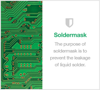
The color that most people are familiar with when it comes to motherboards is green, the color of soldermask. Though not nearly as common, soldermask also sometimes appears in other colors, such as red or blue. Soldermask is also known by the acronym LPISM, which stands for liquid photo imageable soldermask. The purpose of soldermask is to prevent the leakage of liquid solder. In recent years, incidences of this have become more common due to a lack of soldermask. By most accounts, however, users generally prefer boards that have soldermask over boards that don’t.

PCB Solder Mask | PCBCart

Once soldermask has been applied to PCB, the PCB is subjected to molten solder. As this process occurs, exposed surfaces of copper become solderized. The whole process is known as hot air solder leveling (HASL). As SMD chips are soldered, the board is heated to the point where solder takes on a molten form and the components are put into their proper place. As the solder dries, components also become soldered. HASL usually includes lead as one of the compounds in the solder, though lead-free options also exist.

The spacing of track width is indicated by a dash. For instance, when you see the figure 6/6 mils, that would specify 6 mils as the minimum track width, as well as the minimum track spacing. Therefore, all spacing on the board in question should either meet or exceed 6 mils. For those unfamiliar, mils units are used to determine distances on PCB materials. Width and spacing are especially important when it comes to boards that are designed to handle high amounts of current.

When a PCB board is multilayered, various tracks cannot be examined visually for their accessibility. Therefore, a test is performed that places probes at the end of tracks to verify all of the signals are reachable. The test is carried out with applications of volts from one end. If these voltages are sensed from the other side, the tracks are deemed to be in working condition. While the test is not always essential on boards with only one or two layers, it’s still recommended if you truly care about quality.

Vias that connect inner and outer layers are known as blind vias. The name is results from the fact that because such vias can only be spotted from one side. Vias that connect two or more inner layers are known as buried vias, which cannot be spotted from the outside on either side. On boards that contain blind and buried vias, via filling is often used. This keeps the outside surface more secure and helps lower the possibility of solder slipping through and penetrating the inner vias.

Material Selections Affecting Cost

PCB typically costs more when it contains features such as gold tabs, blind or buried vias, or via filling. Likewise, PCB with line / width spacing below 6 mils also tends to cost more. The reason for these higher prices is the alternate process that goes into the production of unusual PCB boards. By the same token, certain PCB productions turn out to be not nearly as profitable or successful when low mils or inner vias are featured, and the higher price is set to recoup losses. Fabricators exist that produce PCB with line / width measurements as low as 3 mils, but this is generally not recommended unless it’s your only option for a particular component.

Power and Heat Impact on PCB Material Selection

Out of all the factors that impact PCBs, two of the most intensive are power and heat. Therefore, it’s crucial to determine the thresholds for each, which can be done by assessing the thermal conductivity of a PCB. This defines how wattage power is turned into temperature through the length of the material. However, there are no established industry-wide values for thermal conductivity.

Power and Heat Impact on PCB Material Selection | PCBCart

For example, Rogers Corp. carries a PCB material, RT/duroid 5880, that is often applied in EW and communications. The dielectric constant of this material is low, as it’s a composite material that contains micro–fibrous glass elements. These microfibers aim to boost strength of the fiber in the material.

Although the PCB is ideal for applications utilize high frequencies, the material’s low thermal conductivity, made it easily heat, which can be a huge drawback in heat-intensive applications.

PCB Materials and Industry Applications

For applications in the military and the aerospace, automobile and medical industries, PCBs are manufactured in single as well as double-sided varieties, some of which are copper clad and others that use aluminum. In each of these industries, the material is used for maximum performance in specific areas. As such, PCB materials are selected their lightweight quality in certain industries or for their ability to handle high amounts of power in others. As such, when performance aptitudes are taken into account, it’s crucial to determine which functions need to be compared with one another when selecting PCB materials, since material levels correlate to performance levels.

Flex and Rigid-Flex Boards

In recent years, flex and rigid-flex boards have grown in popularity because of the options they allow for in a variety of uses. Basically, they can be bent, folded and even wrapped around objects, so they can be used to achieve applications that would never be possible with flat circuit boards. For example, a flex board might be used for a piece of equipment that would require a board to fold at an angle and still carry current from one end to the other without the need for connecting panels.

The majority of flex boards on the market consist of Kapton, a polyimide film that was originated by the DuPont Corporation. The film boasts qualities such as heat resistance, dimensional consistency and a dielectric constant of only 3.6.

Kapton comes in three Pyralux versions:

  • Flame retardant (FR)
  • Non-flame retardant (NFR)
  • Adhesive-less / high performance (AP)

Flex and Rigid-Flex Boards | PCBCart

Selecting PCB Board Materials – Quality First

When it comes to selecting PCB board materials, quality is of utmost importance in the construction of any type of board, whether it’s intended for home electronics or industrial equipment. A component that contains a printed circuit board could be large or small, cheap or expensive, but what matters most is that the item in question offers superior performance for the full duration of its expected lifespan.

PCB Material Selection Guide | PCBCart

While there are several types of PCB materials that go into a given board, product reliability is ultimately what consumers and businesses are looking for in products that use circuit boards. Of course, it’s also crucial that PCB board materials are strong enough to hold together, even if a component accidentally gets dropped or knocked sideways.

On computerized equipment, for example, durable PCBs ensure hardware updates can be made without doing damage to the pre-existing PCB board materials. The same applies to electronics devices, microwaves and other household devices that rely on PCB technology to stay in working condition. Even at electronic public facilities such as ATMs, PCBs must work without fail so buttons will work and commands will be understood without delay.

E3PCB offers a full range of PCB fabrication and assembly services. Thanks to our 10+ years’ experience and innovative technologies, we are capable of handling different laminate materials and substrate materials including FR4, Rogers etc. that are the most popular and widely applied. Our services have been used by engineers across industrial sectors, with unique objectives when it comes to the operation and functionality of components that use PCB.